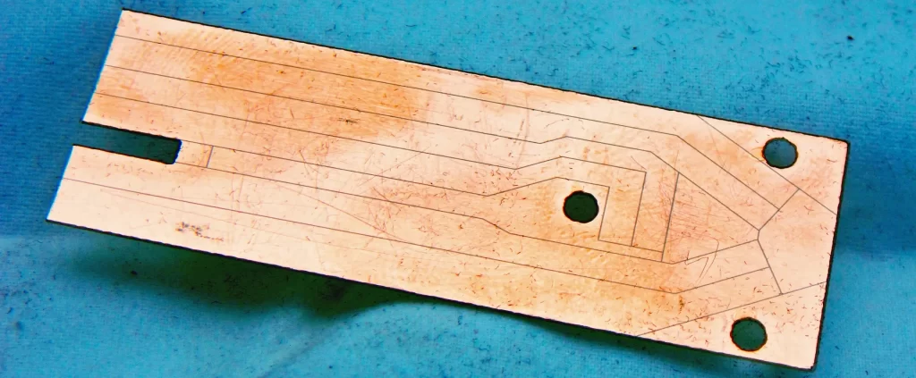
Laser scribing is an optimal solution for defining electrical paths on printed circuit boards (PCBs) due to its precision and efficiency. Unlike traditional methods that rely on photo-sensitive coatings applied to the PCB’s surface, laser scribing directly etches the defined areas with exceptional accuracy. This eliminates the need for additional coating processes, making it a more streamlined and cost-effective approach.
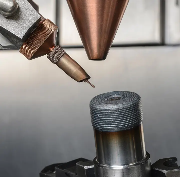
The laser scribing process involves using a focused laser pulse to selectively remove material from the PCB’s surface, creating the necessary electrical paths. This method operates at low laser power, which minimizes thermal impact on the surrounding areas and reduces the risk of damage to the PCB. The precise control of the laser allows for high-definition scribing according to the digital design specified in the software, ensuring that every path is accurately represented.
One of the key advantages of laser scribing technology is its ability to achieve high production rates while maintaining low operational costs. The laser system’s efficiency allows for rapid processing of PCBs, making it suitable for both small and large-scale production runs. Additionally, the absence of additional coatings and the minimal thermal effects contribute to a reduction in overall product costs.
Laser scribing also offers superior flexibility in design. Complex and intricate circuit patterns can be scribed with ease, accommodating a wide range of PCB designs and specifications. This versatility is particularly valuable in industries where precision and customization are paramount.
Moreover, the clean and precise nature of laser scribing ensures that the final PCB product meets stringent quality standards. The process produces high-quality, consistent results with minimal post-processing, reducing the likelihood of defects and enhancing the reliability of the final electronic products.
In summary, PCB laser scribing is a highly efficient and cost-effective method for defining electrical paths on printed circuit boards. By eliminating the need for additional coatings and minimizing thermal effects, this technology offers high production rates, reduced operational costs, and precise results. Its ability to handle complex designs with accuracy and speed makes it an invaluable tool in modern PCB manufacturing.