Table of Contents
- Introduction to Micro-machining
- The Science of Material Response
- Material Response Deep-Dive
- Specialized Application Table
- Actionable Advice for Beginners
- Summary
Introduction to Micro-machining
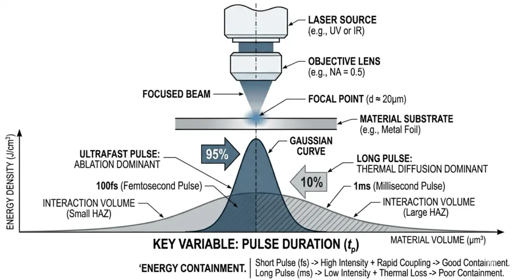
Laser micro-machining is far more than just focusing a powerful beam onto a surface. It is a precise, tailored dialogue between coherent light and the fundamental structure of matter. While optics and raw power are necessary, they are insufficient. The real secret sauce—the parameter that truly dictates precision, throughput, and the viability of an application—is the laser pulse duration.
How a material responds to milliseconds, nanoseconds, picoseconds, and femtoseconds of energy is radically different. Mastering this response means moving beyond a reliance on “cutting speed” or “average power” and developing a nuanced understanding of the dominant physics in play during those critical fleeting moments.
The Science of Material Response
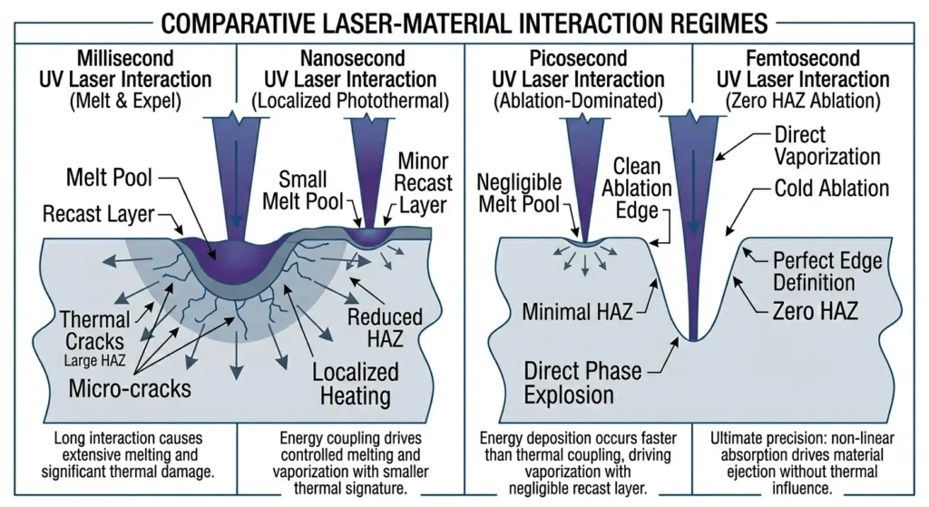
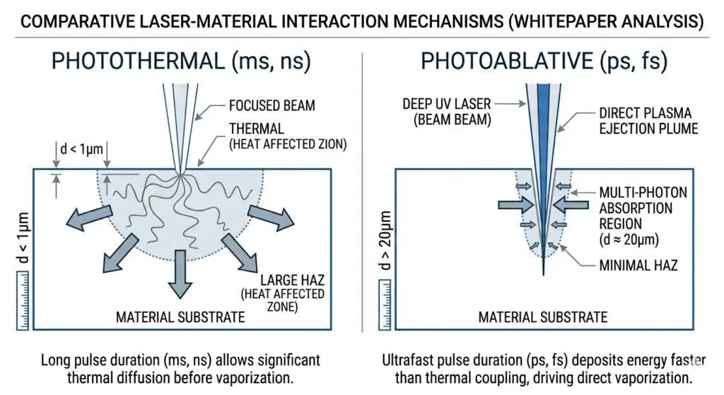
The fundamental challenge in micro-machining is energy containment. We must ask: where does the laser energy go? Does it immediately heat the lattice, creating a large, problematic melt pool, or is it trapped by electrons, driving direct vaporization? This question defines the Heat Affected Zone (HAZ).
The Dominant Regimes
The material response divides broadly into two regimes:
- Photothermal (ms and ns): The laser pulse is long enough that photons are absorbed, converted to heat, and conduct significantly into the bulk material before vaporization begins. The material melts, boils, and expels.
- Photoablative (ps and fs): Also called “cold ablation,” these ultra-short pulses deposit energy faster than the electron-phonon coupling time. Non-linear absorption mechanisms, such as multi-photon absorption, become dominant. The energy is deposited almost instantaneously, driving a direct phase transition to a plasma, with minimal or no significant thermal diffusion.
New Frontiers in 2021–2026
Recent advancements between 2021 and 2026 have refined our understanding. In critical aerospace alloys and biomedical magnesium, picosecond pulses (10–50 ps) have shown a unique ability to minimize the formation of chaotic recast layers, offering a significant surface quality improvement compared to standard nanosecond approaches (especially at 1064nm).
A major recent breakthrough is the industrial rise of GHz Burst Mode for ultrafast (fs and ps) lasers. Traditionally, ultra-short pulses faced an “ablation cooling” limit—where subsequent pulses in a pulse train were too slow to benefit from previous interactions. GHz bursting delivers pulses in incredibly tight sequences (e.g., eight pulses within nanoseconds), bypassing this limit. This allows operators to achieve near-photoablative quality but with significantly higher volumetric throughput, especially in brittle advanced ceramics like alumina and zirconia, without inducing micro-cracking.
Material Response Deep-Dive
Millisecond (ms): The Melting Power
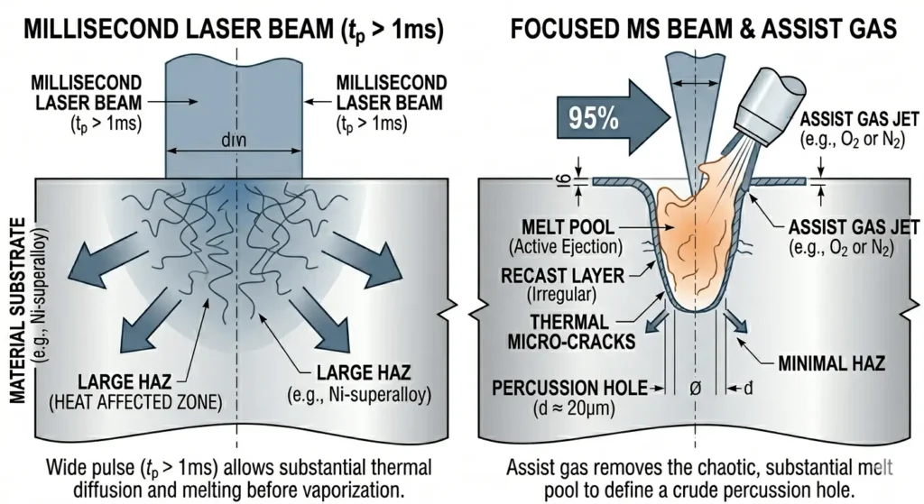
This is micro-machining’s equivalent of a heavy hammer. Millisecond pulses are long enough to drive substantial melting. The primary interaction mechanism is photothermal. When drilling cooling holes in single-crystal superalloys for aerospace engines, the goal is often speed. The millisecond pulse melts the material, and high-pressure assist gas (often O2 or N2) blows the melt out.
The trade-off is unavoidable. A significant HAZ will develop, and a recast layer (resolidified melt material) will line the cut. Surface finishes are often rough and require post-processing. Control is challenging; you cannot easily define a complex 3D shape with melting physics.
Nanosecond (ns): The Industrial Workhorse
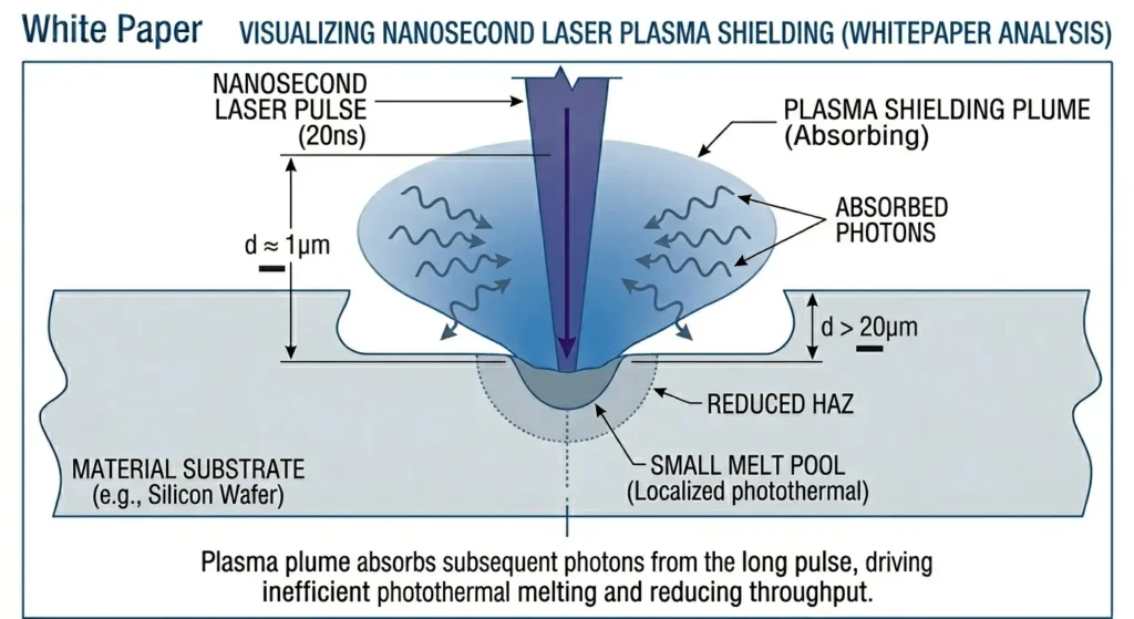
For decades, the nanosecond laser has been the global micro-machining standard. Nanosecond pulses still operate primarily photothermally, but the shorter duration (5-200 ns) localizes the interaction. There is less time for thermal conduction than in the ms regime.
However, plasma shielding is a major limitation. The initial photons generate a plasma plume that absorbs much of the subsequent pulse energy, reducing efficient processing. This results in melt expulsion as the dominant removal mechanism, often leaving a messy edge. The HAZ is smaller than millisecond machining but still substantial—around 10-50 µm depending on the metal and wavelength (532nm or 1064nm are common). If a perfect 180°C operating window or a surface finish of 0.2 µm Ra is required, ns is likely the wrong choice.
Picosecond (ps): The Precision Bridge
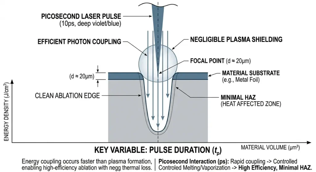
Entering the picosecond (ps) regime moves us toward true precision. A 10–20 ps pulse is shorter than the typical thermal coupling time for metal. This creates a bridge between photothermal melting and cold ablation.
While some thermal effects persist, they are dramatically reduced. The HAZ is often sub-micron. Recent work on aerospace engine blades has confirmed that picosecond drilling of complex hole profiles results in vastly cleaner edges and a negligible recast layer compared to ns drilling. This precision makes picosecond lasers suitable for thin-film patterning (like in perovskite solar) and complex sapphire substrate modification.
Femtosecond (fs): The Ultimate Cold Cut
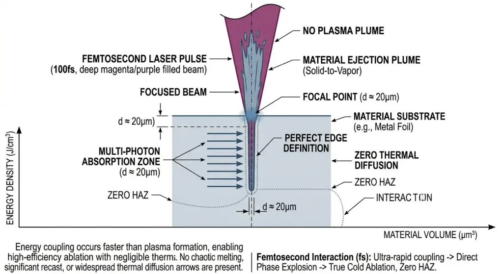
This is the peak of cold ablation. The pulse duration (100–900 fs) is so incredibly brief that the energy is deposited within a material volume much faster than the thermal wave can diffuse. The electrons are excited to a very high energy state, and non-linear absorption mechanisms allow materials that are normally transparent (like glass or polymer) to strongly absorb the energy.
This results in direct vaporization. The material transitions from solid to gas and plasma without passing through a significant liquid phase. The result? Zero thermal damage. No melting, no recast layer, no micro-cracking. For nitinol stents (the quintessential femtosecond application), fs lasers eliminate the risk of thermal fatigue failure and the need for expensive post-laser finishing steps like electrochemical polishing. The throughput limits of fs lasers have been the classic bottleneck, but GHz Bursting is rapidly resolving this.
Specialized Application Table
The following table details 15 highly complex micro-machining applications requiring a specific material response.
| Laser Type | Interaction Mechanism | Specialized Application & Description | Why It’s Suitable |
| Millisecond | Photothermal (Melt/Expel) | Percussion Drilling (Aerospace) | High-speed drilling of cooling holes (<0.5mm dia) in single-crystal Ni-superalloys for engine blades. |
| Nanosecond | Photothermal | TFT Circuit Repair (Semiconductor) | Selective metal ablation of shorted circuit paths (1-5µm width) on flat-panel displays. |
| Femtosecond | Photoablation (GHz Burst) | Nitinol Stent Profiling (MedTech) | Creating complex geometry and strut patterns in shape-memory nitinol (NiTi) tubes for cardiac stents. |
| Picosecond | “Cold-Edge” Photothermal | Perovskite Solar Scribbing (Renewable Energy) | Clean patterning of P1, P2, and P3 layers (<20µm width) on thin-film photovoltaic stacks. |
| Femtosecond | Non-Linear Absorption | Internal Glass Microfluidics (Bio-photonics) | Creating hidden, complex 3D network channels and reservoirs inside bulk borosilicate glass. |
| Femtosecond | Direct Phase Explosion | Orthopedic Implant Texturing (MedTech) | Texturing the surface of titanium alloy implants (Ti-6Al-4V) to optimize osseointegration. |
| Picosecond | “Cold-Edge” Photothermal | Selective Laser Etching of Sapphire (ps) | Patterning complex, multi-micron-deep features for optical filters or LED substrates. |
| Nanosecond | Photothermal | Copper Trace Trimming (Electronics) | Precision adjustment of trace resistance in complex RF circuits and dense PCBs. |
| Femtosecond | Non-Linear Absorption | Quantum Hardware Qubit Patterning (Quantum) | Patterning superconducting qubit circuits (e.g., Al/AlOx/Al) with sub-micron resolution on silicon or sapphire. |
| Picosecond | “Cold-Edge” Photothermal | Ceramic Micro-Vias (Advanced Packaging) | Drilling sub-100µm micro-vias through thin ceramic interposers for advanced semiconductor packaging. |
| Nanosecond | Photothermal (Melt/Expel) | Scribing of Thin-Film CIGS Solar Cells | Making P1, P2, and P3 electrical isolation scribes across CIGS photovoltaic materials. |
| Femtosecond | Photoablation (GHz Burst) | Scribing Brittle Diamond Heat Spreaders | High-throughput cutting and shaping of synthetic diamond (CVD diamond) heat spreaders. |
| Femtosecond | Non-Linear Absorption | Marking Traceability Data on PMMA Lenses (MedTech) | Applying serialized text and barcodes to the non-optical edge of intraocular lenses (IOLs) made of PMMA. |
| Picosecond | Plasma-Coupling Photothermal | Selective Metal Thin-Film Ablation (Photomask) | Precise modification of chromium or metal-silicide thin-film patterns on glass photomasks. |
| Millisecond | Photothermal (Melt/Expel) | Multi-layered Composite Percussion Drilling | Rapidly drilling hundreds of small diameter holes in carbon-fiber reinforced polymer (CFRP) panels for acoustic liners. |
Pro-Tip: When to Shorten the Pulse Are you struggling with chaotic material response? If you see a large melt pool, micro-cracks, or a rough edge, don’t increase the average power—this usually just increases the damage. Instead, shorten your pulse duration. For high thermal conductivity metals (like gold or copper), moving to the ps or fs regime is often non-negotiable for precision, as heat travels incredibly fast. For low thermal conductivity polymers (like PMMA), you can often get away with a ns green (532nm) system, but if you need a zero-debris cut, fs is your only path. Think about your material first, not your laser.
Actionable Advice for Beginners
1. Know Your Target’s Thermal Signature
The material’s response starts with its basic properties. If you are working with a material that is highly thermally conductive (like copper or gold) and requires precision, you must prioritize the ultrafast regimes (fs or ps). The energy must be applied faster than the material can carry it away. Nanosecond pulses on copper just lead to messy melting and plasma shielding.
2. Don’t Pay for Overkill
Ultrafast (fs/ps) lasers are the ultimate cold tools, but they carry a high price tag. For simple drilling, scribing, or marking on non-brittle materials (like many standard plastics or thick stainless steel), a robust nanosecond system will often achieve the required 10-20 µm edge tolerance at a fraction of the capital and operational cost.
3. Consider Surface Finish as Your First Metric
Is a 0.5 µm Ra (roughness average) the primary specification? Then your choice is effectively limited to fs, ps, or high-performance ns using specialized assist gases. If 20 µm Ra is acceptable, millisecond lasers using percussion techniques are the clear winner for throughput. The surface finish requirement is often the most accurate guide to the dominant interaction regime you must select.
Summary
The final application requirement (HAZ, surface roughness, throughput) always dictates the necessary laser regime.
Laser micro-machining is not just energy delivery; it is tailoring the material response (photothermal vs. photoablative).
Pulse duration (ms, ns, ps, fs) is the parameter that most strongly controls this response andEnergy containment.
Recent breakthroughs (2021–2026) like GHz Burst Mode have enabled fs/ps lasers to achieve high throughput in ceramics, while ps lasers offer a precision bridge minimizing recast layers.